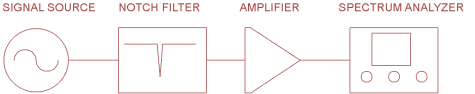
Measuring phase noise is difficult, due to the large difference between the signal and the noise. Here I will outline the method I use to determine the noise of a oscillator and show the basic bandpass – notch filter used to reduce the carrier level to a level that the common spectrum analyzer can handle. The filter shown here will be made for 9MHz, but other frequencies can be realized as long as high Q matched crystals can be found.
When doing these measurements, reducing the noise figure of the spectrum analyzer, and knowing the inserted gain is important. I use a module with a ERA-2 MMIC mounted in a die cast box with extended filtering on the DC input.
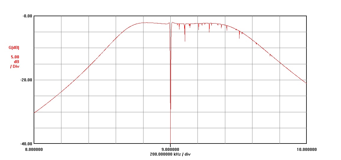
The filter module start with a QTC (Quad Tuned Circuit) mixed form bandpass filter. This is built and tuned for a flat bandpass before the notch

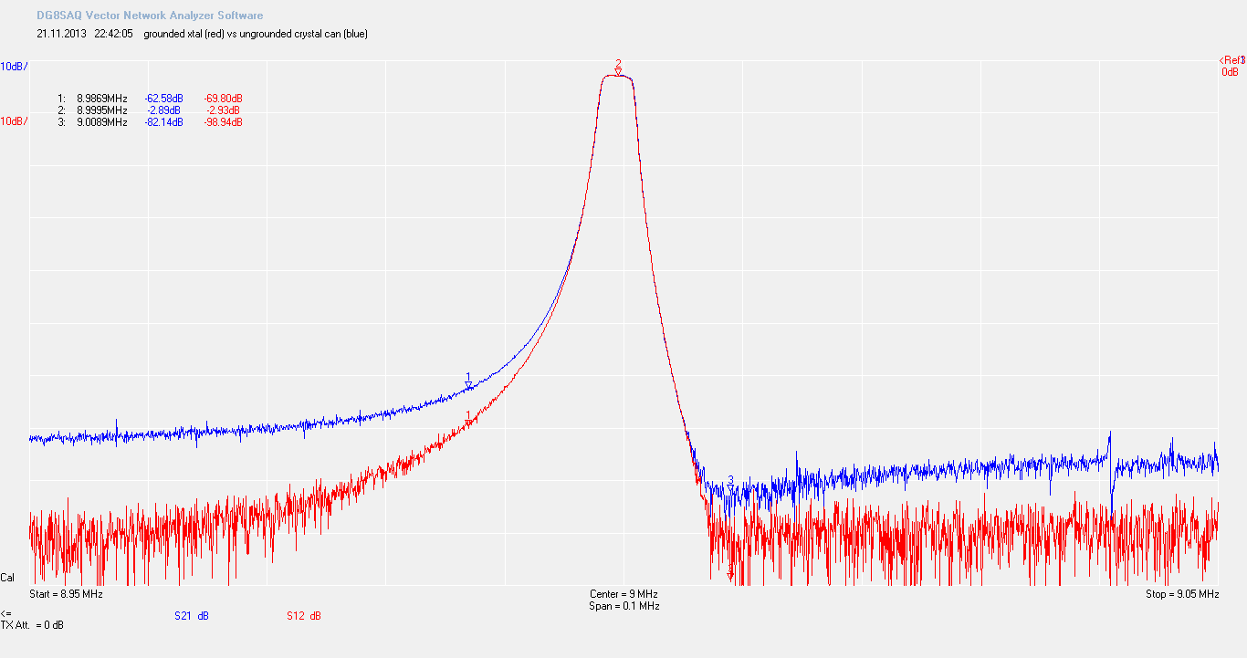
After the filter is built and tuned the crystals are connected over the 2 resonators in center and the filter is adjusted to have a as flat as possible passband. This way, with crystals matched as close as possible (2Hz) the notch depth should be better than 80dB. If the crystals can’t be matched, then a trim capacitor can be placed in series with the crystal, but this makes the tuning of the notch depth much more difficult.

The obtained filter does not need to have the notch in the center of the passband. the 3dB points of the filter will be what limits the bandwith of your measurement. If the crystals have high Q and no spurious responces (mine had some) then the passband should be flat. If there is some spurious responces, you can average it out on most spectrum analyzers. Knowing the width of the notch at the 3dB point determines how close to the carrier you can measure the phase noise.
To use the filter with a spectrum analyzer, you add a low noise amplifier with known gain at the frequency you operate on between the filter and the spectrum analyzer. Add a variable attenuator in front of the filter and set this to max attenuation before connecting it to the signal source.
Tune the signal source to the frequency where it is attenuated the most by the filter and reduce the attenuation to 0. If The noise level around the notch should be somewhat higher than the attenuated carrier.
If the spectrum analyzer have a marker that can show the amplitude level in dBm/Hz then the level of the phase noise in dBc is: Source output power(dBm) + noise amplitude (dBm) + (loss through filter in dB) – (amplifier gain in dB). For example, lets assume my source is at 10dBm, the measured noise level at -115dBm, 2.4dB filter loss and 20dB gain: 10dBm + (-115dBm/hz) + (-2.4dB) – (20dB) = -127dBc/Hz phase noise.
If the analyzer does not have a marker function then you need to know the bandwith of the IF filter in the analyzer in addition to the parameters above. The total equation would then be: Source output power(dBm) + noise amplitude (dBm) + (loss through filter) – (amplifier gain) – 20*log(analyzer bandwith in Hz ). For example, source at 10dBm, measured noise level at -105dBbm in 100Hz bandwith, 2.4dB filter loss and 20dB gain: 10dBm + (-95dBm) +(-2.4dB) – (20dB) -(20*log(100)) = -147dB/Hz phase noise.
Accurate noise measurements are not easy to do. Careful evaluation of all used components and careful measurements with averaging of the traces helps to obtain accurate measurements. Alternative methods use phasing or PLL methods, and have better accuracy over a larger bandwidth, at the expence of a more advanced measurement setup.
Update 1.th February 2015:
Did a measurement of the HP8656B signal generator using the notch filter and a ERA-2 amplifier with 15.7dB gain:

The input signal into the notch filter were 0dBm and the notch filter loss 2.4dB. The total equation will then be: 0 +(-106.1dBm/Hz) + (-2.4dB) -15.7dB = -124.2dBc/Hz at the point 10KHz offset from the carrier. This value corresponds well with other methods used to measure the phase noise on this generator. The value is 10dB better than the than what the datasheet states as worst case phase noise, not uncommon for HP equipment from the 1980s era.