NIST on phase detectors and some verification.

NIST has some interesting articles on their website, one of them being a 5 MHz phase detector with low residual flicker [1] for measuring phase noise.  This spurred some discussions and a series of measurements on my part.

mixer_pd_sch

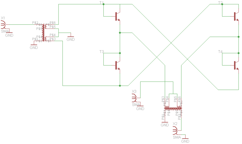
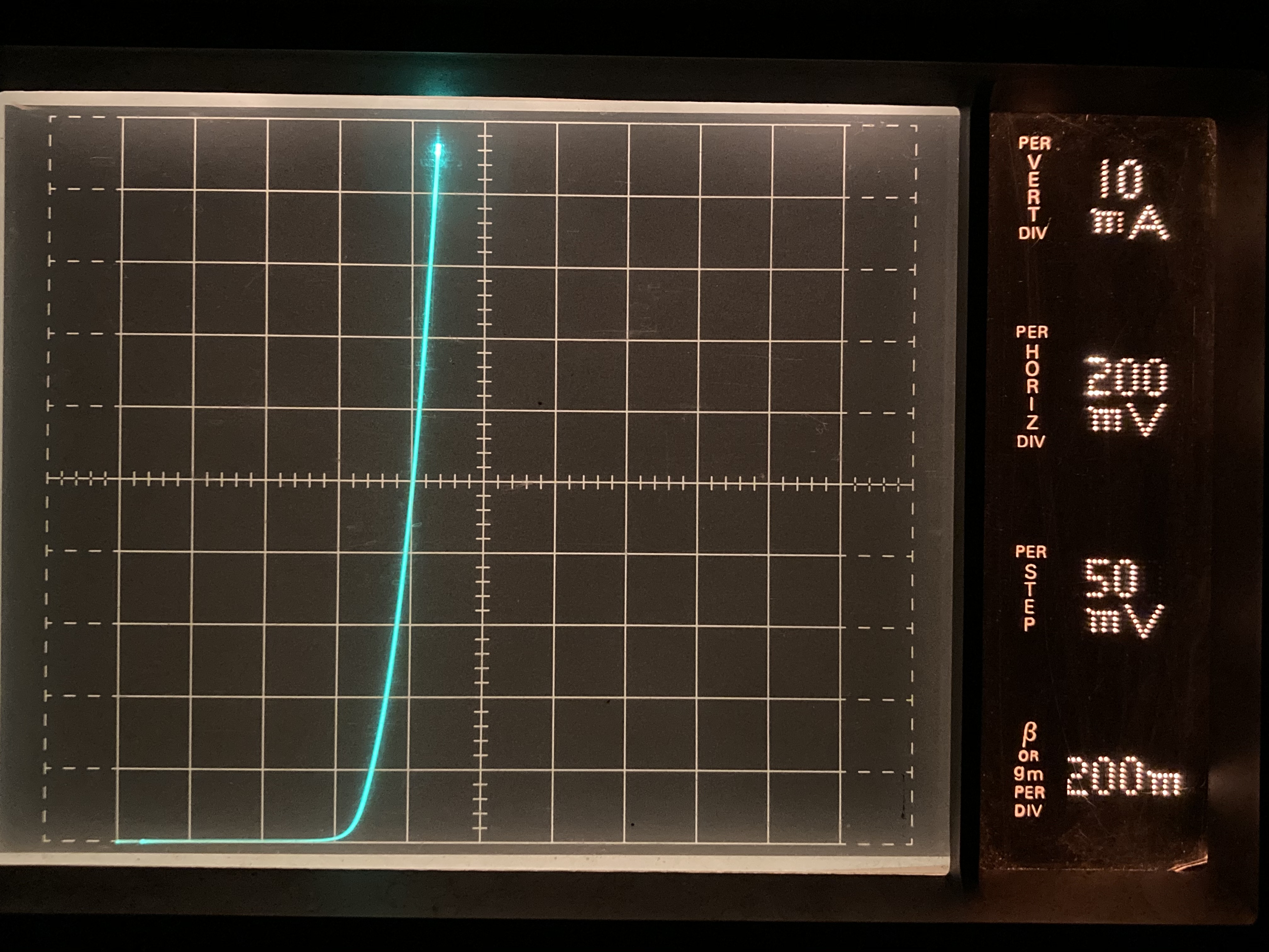
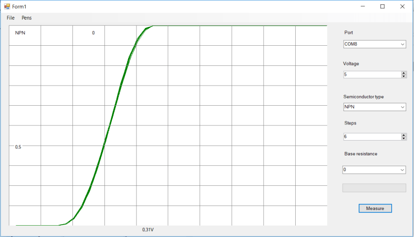
The interesting part is the usage of common 2N2222 transistors.  There have been some discussion on the internet about the outlined connection of the transistor as a diode with the BC junction shorted. Some claiming it behaving as a switch, while others claiming it to be a diode. My own suspicion was that this would act as a diode, and a mixer was built tusing BC547B’s.  A quick look at my crude curve tracer shows the diode action:

ct_diode_bc547

The mixer uses a 5:1 transformer for optimal impedance match, and I was not able to find a pair in my junkbox.  Using FT-2402-43 cores, with a 2t primary, and a bifilar 4.5 turns secondary winding. 4 diode connected transistors and the mixer is working.

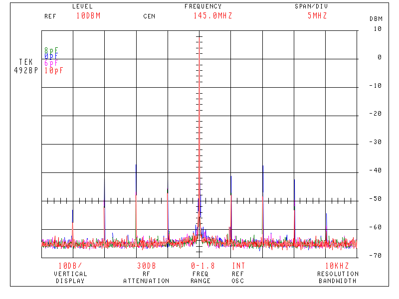
Mixing action was verified on a spectrum analyzer before compression points were measured used the 30% am technique.

compression_bc547mixer


As can be clearly seen, as long as the diodes are conducting, the mixing action is linear.  With the low LO amplitude of 0dBm, the diodes are not conducting properly and that can be shown on the plot of the linearity. Notice that the mixer is in compression with as low as -8dBm input level. The bend and slope with 17dBm LO is somewhat larger than for the lower amplitudes, indicating that the mixer LO may be excessive. Some spectrum analyzer plots showing the IMD products should give further insight into this, if used as a mixer.

nist_mix_spectr

As a last test, I did try to use this phase detector to measure phase noise, using my current setup.  Unfortunately there was little change compared to the much more noisy level 7 mixer it has. This is due to the noise in the low noise amplifier that follows the phase detector and masks any improvement in the phase detector for now.  A new, 100pV/sqrt Hz input noise amplifier is planned.


[1] https://tf.nist.gov/general/pdf/2554.pdf


Note 18 nov 19:

Did a measurement of IL vs LO level at different frequencies:

IL_NIST

Note 22 june 2020:

Si5351 Spurius preformance

As some of you know, I have done a lot of work with the Si5351 series of synthesizers. In a couple of blog post, I will try to document some of the more subtile details of operation of this chip. Since I don’t have access to the actual mask sets for the chips some of these statements are qualified guessing, based on observations by NT7S and myself.

I believe the routing in the chip to be more complicated than outlined in the datasheet. Trying to determine where the spurious responses come from, and why they have their amplitudes have shown some of the internals that I will try to outline. Lets start with the block diagram, shamelessly stolen from SiLabs:

si5351abc_block

The Synthesizer consists of a crystal oscillator (or TCXO/OCXO) with drivers. The performance of this is depending on the signal quality. A good designed crystal oscillator with a limiter will outperform the internal oscillator on phase noise.  Notice that the C version has a switching matrix after the oscillator and the option to feed in an external clock. This is a nice option for those cheap OCXO’s that are on non-integer frequencies.

A bit interesting is it that the datasheet mentions 25MHz and 27MHz as the alternative frequencies, but the chip works on a broad range. That 26MHz crystal will work just fine. I do believe the input frequency are divided down to  5MHz, before being distributed internally. This would then be routed out to PLL A and B, microcontroller (for the I2C) and probably to the multisynth stages as a clock.

There are both internal and external capacitors to the device. A interesting point is that when using regular crystals the spurious products seems to be reduced when selecting the internal capacitors, unlike loading with external capacitors.

overlay_si5351b2

The above picture is taken with PLL A set to 870MHz and the multisynth set to 6. There is up to 10dB difference between the 0pF (blue plot) and 10pF (red plot), using the internal capacitors. Selecting the 0pF internal capacitor, and using external 18pF, lead to a 10dB increase in spurs above what can be seen above. I should point out that while there are some spurs, they are not a deal breaker in this case, the above spurs can easily be removed by bandpass filtering if necessary.

The PLL’s seems to be a fairly common design, with a PLL bandwidth of around 200KHz (there are some subtile spurs). The PLL operates over the range 600MHz-900MHz. This part is the well-behaved part of the chip.

The “Multisynth” is the unknown part of the chip. I believe this is some kind of fractional divider,  clocked by the PLL signal and the 5MHz internal clock. The output spurs are reduced when the divider is operated at integer divisions instead of fractional divisions. Some experiments suggest that the multisynth is followed by a divide-by-2, as the output always have a 50% duty cycle square wave.

The way to get the best performance is to lock the Multisynth at a suitable integer level, and move the PLL to do the frequency change.  The output should be used with a switching type mixer (DBM with diodes in saturation or switches) in order to get the best preformance. A good limiter could reduce the spurious responses, perhaps reducing the voltage to the output buffer would help in driving them deeper into saturation, and giving better limiting action?

ADDITION 31. dec 16: The above plot is the worst case I have been able to make by abusing the Si5351. This is not at all typical performance. The 200KHz spurs is usually found at an amplitude less than -110dBc, and other spurious products should be below -70dBc. In my opinion, the chip is well suited as local oscillator in a receiver. 

A notch filter for phase noise measurment

Measuring phase noise is difficult, due to the large difference between the signal and the noise.  Here I will outline the method I use to determine the noise of a oscillator and show the basic bandpass – notch filter used to reduce the carrier level to a level that the common spectrum analyzer can handle.   The filter shown here will be made for 9MHz, but other frequencies can be realized as long as high Q matched crystals can be found.

When doing these measurements, reducing the noise figure of the spectrum analyzer, and knowing the inserted gain is important. I use a module with a ERA-2 MMIC mounted in a die cast box with extended filtering on the DC input.

The filter module start with a QTC (Quad Tuned Circuit) mixed form bandpass filter.  This is built and tuned for a flat bandpass before the notch

QTC_9MHz

After the filter is built and tuned the crystals are connected over the 2 resonators in center and the filter is adjusted to have a as flat as possible passband. This way, with crystals matched as close as possible (2Hz) the notch depth should be better than 80dB. If the crystals can’t be matched, then a trim capacitor can be placed in series with the crystal, but this makes the tuning of the notch depth much more difficult.

QTC_9MHz_notch

The obtained filter does not need to have the notch in the center of the passband. the 3dB points of the filter will be what limits the bandwith of your measurement. If the crystals have high Q and no spurious responces (mine had some) then the passband should be flat. If there is some spurious responces, you can average it out on most spectrum analyzers. Knowing the width of the notch at the 3dB point determines how close to the carrier you can measure the phase noise.

notchfilter

To use the filter with a spectrum analyzer, you add a low noise amplifier with known gain at the frequency you operate on between the filter and the spectrum analyzer. Add a variable attenuator in front of the filter and set this to max attenuation before connecting it to the signal source.

Tune the signal source to the frequency where it is attenuated the most by the filter and reduce the attenuation to 0. If The noise level around the notch should be somewhat higher than the attenuated carrier.

If the spectrum analyzer have a marker that can show the amplitude level in dBm/Hz then the level of the phase noise in dBc is: Source output power(dBm) + noise amplitude (dBm) + (loss through filter in dB) – (amplifier gain in dB). For example, lets assume my source is at 10dBm, the measured noise level at -115dBm,  2.4dB filter loss and 20dB gain:  10dBm + (-115dBm/hz) + (-2.4dB) –  (20dB) = -127dBc/Hz phase noise.

If the analyzer does not have a marker function then you need to know the bandwith of the IF filter in the analyzer in addition to the parameters above.  The total equation would then be: Source output power(dBm) + noise amplitude (dBm) + (loss through filter) – (amplifier gain) – 20*log(analyzer bandwith in Hz ).   For example, source at 10dBm, measured noise level at -105dBbm in 100Hz bandwith, 2.4dB filter loss and 20dB gain: 10dBm + (-95dBm) +(-2.4dB) – (20dB) -(20*log(100)) = -147dB/Hz phase noise.

block_phasenoise

Accurate noise measurements are not easy to do. Careful evaluation of all used components and careful measurements with averaging of the traces helps to obtain accurate measurements. Alternative methods use phasing or PLL methods, and have better accuracy over a larger bandwidth, at the expence of a more advanced measurement setup.

Update 1.th February 2015:

Did a measurement of the HP8656B signal generator using the notch filter and a ERA-2 amplifier with 15.7dB gain:

notchfilter_9MHz_HP8656B


The input signal into the notch filter were 0dBm and the notch filter loss 2.4dB. The total equation will then be: 0 +(-106.1dBm/Hz) + (-2.4dB) -15.7dB = -124.2dBc/Hz at the point 10KHz offset from the carrier.  This value corresponds well with other methods used to measure the phase noise on this generator. The value is 10dB better than the than what the datasheet states as worst case phase noise, not uncommon for HP equipment from the 1980s era.