NanoVNA linearity

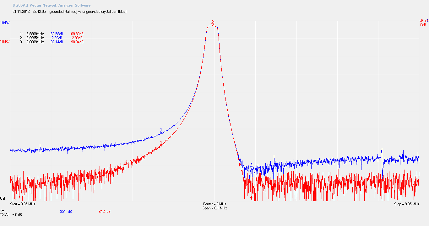
Over the past few months, considerable work has been done with the NanoVNA, an excellent compact vector network analyzer that performs well up to around 300 MHz. However, the available dynamic range is somewhat limited, comparable to that of an HP8410 at 10 GHz. The following measurements were performed to evaluate an original NanoVNA-H4.

One challenge encountered was when measuring amplifiers. For a portion of the amplifier’s range, there was clear evidence of compression. But was it the VNA, the amplifier, or some other factor causing it? This led to the development of a setup to measure the compression point of the NanoVNA.

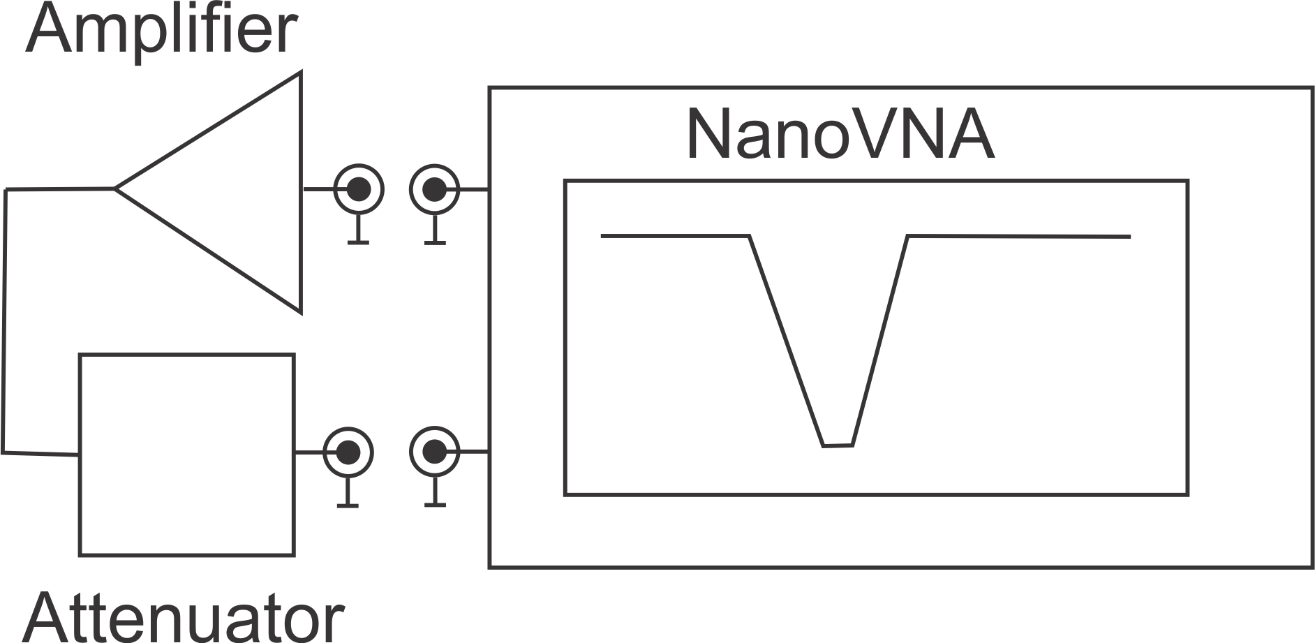
The setup included the NanoVNA, calibrated using a SOLT (Short, Open, Load, Through) procedure, with the shortest possible coaxial cable to ensure a 0 dB S21 response. A proper amplifier (Mini-Circuits ZFL-1000H) was used, terminated with a 6 dB attenuator, followed by a programmable attenuator. The amplifier’s output was measured at a single frequency while adjusting the attenuator. This ensured that the input level to the amplifier and the impedance remained consistent across all measurements, minimizing inaccuracies.

A Python script controlled the process, automating the reading of the NanoVNA, adjusting the attenuator, and taking new measurements. The NanoVNA’s power mode was set to “AUTO” during these measurements, as it was found to provide more consistent power compared to manual output settings.

The results are as follows:

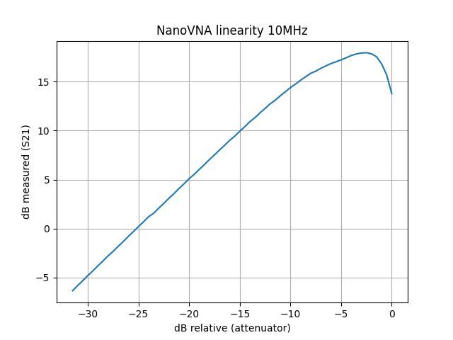
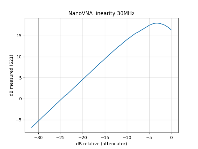
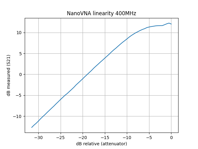
The data is plotted with the attenuator value on the X-axis and the measured output on the Y-axis. At HF frequencies, the results were satisfactory. It is generally safe to measure an amplifier with up to 10 dB gain connected directly to the VNA, but for amplifiers with higher gain, either the VNA’s output power should be reduced, or an external attenuator should be used on port 2. Above 200 MHz, there was little change in the compression point until around 300 MHz, where the VNA begins using the third harmonic for detection. As expected, this resulted in a lower compression point.

The disappointing part occurred above 600 MHz, where the VNA relies on the fifth harmonic. Here, the compression point decreased with increasing frequency. Interestingly, there was a specific power level at which the reported output was -24 dB. This value was consistently observed, and after multiple tests with different amplifiers and attenuators, it was determined to be an actual response of the NanoVNA, not a measurement artifact.

For those using the NanoVNA to measure amplifiers, it is recommended to proceed with caution when dealing with amplifiers that have high gain. Be sure to adjust the VNA’s output power or include external attenuation to avoid distortion in the measurements.

Any benefit to grounding crystal cases?

An while ago, I was asked about if there was any benefit to ground the crystal case when using them in ladder filters. I provided an quite simplified analysis and a VNA picture. After some more thinking about it I decided to extend the analysis, as the simplified version does not cover it complete.

The crystal model we use is an simplification into known components that makes the analysis of the crystal possible with easy means:

crystal


An extension of this model is to extend the capacitor C0 into 3 capacitors.

crystal_expanded


The series resonance consisting of Lm, Cm and ESR can for frequencies outside the resonance range, be assumed to be high impedance and can be somewhat simplified to an voltage divider.

Crystal_simplification

By grounding the case of the crystal, the capacitor C1 and C2 gets added to the shunt capacitors for the filter, while when the case is ungrounded the series connection of the capacitors add to the capacitor C0, leading to more of the signal leaking through at the stop-band.

A sweep from an VNA of a filter ungrounded (blue) and grounded (red) show how the stop-band attenuation changes

xtal_isolation

By taking a couple of measurements off several common HC49 528MHz crystals, I obtained the following results: C0=3.4pF, C1 = 2pF, C2=2.1pF.

This data correspond quite well to the rule used by several experimenter of C0=220Cm+1pF. The 220Cm part is due to the physics of the AT cut crystal. An different crystal will have different constants due to the physics of the crystal. The 1pF will be the result of the series connected capacitors C1 and C2.

As this simple analysis show, there is a benefit to ground the crystals. Most modern crystals are welded, and you will need quite a lot of heat to do damage to the crystal, while older crystals may be soldered. The stability of the crystal will be depending on the atmosphere inside the crystal. Some crystals change their parameters quite a lot when opened, while others don’t change at all, so avoid soldering directly to the old style crystals.

open T-check

As of 24 mar 2018, I will no longer do any updates to the T-check program, I reccomend you try out KE5FX’s GPIB toolkit, as this has a similar program.

Ok, since this blog seems to be about the software I write, and not about RF engineering, altough this may be related.

T-check is an routine by R&S to verify the validity of network analyzer SOLT calibration.  This is explained in the R&S application note 1EZ43_0E, covering the math behind the routine as well as the T-checker, an coaxial adapter with an integrated 50 ohm resistor. An simplified method to realize this may be an T adapter with an 50 ohm termination on the 3. port.

t-check

The VNA is calibrated and this device is inserted instead of the DUT. The S-parameters are then saved and run through the T-checker program.

t-check

The program, as supplied from R&S does only work on 32bit computers.  I made an implementation that run on both 64bit and 32bit windows as well as linux, BSD, UNIX, OSX and even Playstation 3 with MONO.

My implementation, named “open T-check” are avaible here