Any benefit to grounding crystal cases?

An while ago, I was asked about if there was any benefit to ground the crystal case when using them in ladder filters. I provided an quite simplified analysis and a VNA picture. After some more thinking about it I decided to extend the analysis, as the simplified version does not cover it complete.

The crystal model we use is an simplification into known components that makes the analysis of the crystal possible with easy means:

crystal


An extension of this model is to extend the capacitor C0 into 3 capacitors.

crystal_expanded


The series resonance consisting of Lm, Cm and ESR can for frequencies outside the resonance range, be assumed to be high impedance and can be somewhat simplified to an voltage divider.

Crystal_simplification

By grounding the case of the crystal, the capacitor C1 and C2 gets added to the shunt capacitors for the filter, while when the case is ungrounded the series connection of the capacitors add to the capacitor C0, leading to more of the signal leaking through at the stop-band.

A sweep from an VNA of a filter ungrounded (blue) and grounded (red) show how the stop-band attenuation changes

xtal_isolation

By taking a couple of measurements off several common HC49 528MHz crystals, I obtained the following results: C0=3.4pF, C1 = 2pF, C2=2.1pF.

This data correspond quite well to the rule used by several experimenter of C0=220Cm+1pF. The 220Cm part is due to the physics of the AT cut crystal. An different crystal will have different constants due to the physics of the crystal. The 1pF will be the result of the series connected capacitors C1 and C2.

As this simple analysis show, there is a benefit to ground the crystals. Most modern crystals are welded, and you will need quite a lot of heat to do damage to the crystal, while older crystals may be soldered. The stability of the crystal will be depending on the atmosphere inside the crystal. Some crystals change their parameters quite a lot when opened, while others don’t change at all, so avoid soldering directly to the old style crystals.

IMD measurment generator

IMD or Intermodulation distortion testing is in RF systems usually done with 2 signal sources, quite close in frequency, and one determines the level of the unwanted responses. The actual measurement procedure is shown quite well other places in the literature [1].

Here I will show my design for an high performance crystal controlled RF source delivering 100mW or so into 50 ohm at HF. The obtained phase noise from this generator are better than the resolving bandwidth of my phase noise measurement -140dBc so there should not be any problems from the phase noise of the signals.

final_schematic

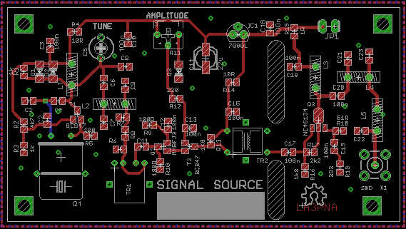
The oscillator circuit used is an common base Butler circuit, as described in Matthys [2]. There are a total of 5 frequency dependent components, the crystal, the inductor, and 3 capacitors. The oscillator have limiting to reduce the oscillation amplitude and to improve the frequency drift.

values

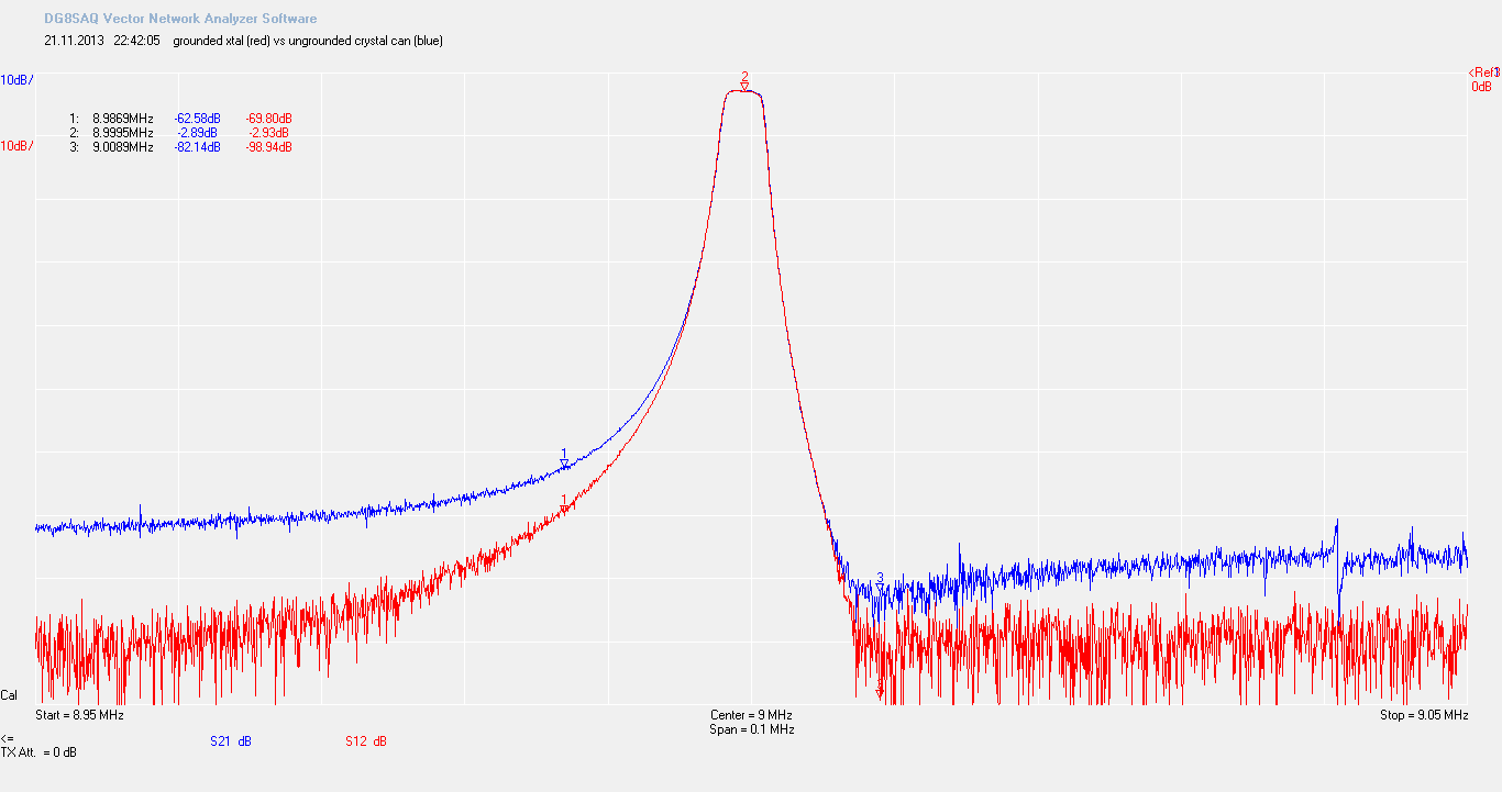
C5+C8 is selected such that the middle value falls in the center of the trimmer C5 range. The chosen crystal should be an HC49 size, not one of the smaller models, as those tend to drift more than their larger counterparts. Measured drift for this oscillator on 3.7MHz is less than 10Hz from start (red trace). Crystals can be ordered from [3] or [4]. Crystal ovens are not recommended, if temperature drift is a problem, fit the crystal with an Styrofoam bead to insulate.

grr_drift

The oscillator is followed by an 3. order low-pass filter to remove harmonic products from the limiting of the oscillator. There exists several types of filter one can use if one wants, I have calculated the values for an half wave filter. This have the simplicity of calculation that the reactances of the components are equal to the system impedance. In this case, for an given frequency :

formula1
where f is the crystal operating frequency in Hz. Different filter topologies like Chebychew or Butterworth can be used to improve the harmonic attenuation of the filters. Information on the calculations of such filters can be found in [1]

Following the filter is an attenuator that can be inserted if the max output level is higher than the desired operating amplitude. Suitable attenuator values can be found several places on the internet. If not used, insert an 0 ohm resistor into R8.

The attenuator is followed by an variable gain hybrid cascade amplifier. This consists of an cascade of an J-fet (MMBT310) and an bipolar transistor (BC847). The J-fet is impedance matched to the 50 ohm system with an balun made by winding 4 turns bifilar on an BN-43-2402 ferrite binocular core. The output is in an similar way matched to the power amplifier with an transformer wound on an BN-43-2402 core. The primary side against the hybrid cascade consists of 12 turns, the side against the power amplifier consists of 2 turns. Wind these such that the leads protrude on each side of the core. The amplifier gain can be adjusted with the trimmer R11 such that the output amplitude is at an fixed level, or this can be taken to an potentiometer mounted in the box such that the output power can be varied if needed.

The power amplifier consists of an NE46134 medium power RF transistor, operating in class AB and delivering a nominal 100mW output power. The inductor is wound on an FT37-43 ferrite core, and 10 turns should suffice for all HF frequencies. Following this is an 5.th order low-pass filter. This filter uses the same capacitor and inductor values as calculated for the 3. order filter before. Observe that C23 is double the value of the other capacitors. The inductors should be wound on iron core toroids. T37 size is recommended. -2, -7 and -10 material should fit the frequency range from 2MHz to 50MHz.

IMD_source_plot

final_board

The PCB for this design is available from OSHpark:

https://oshpark.com/shared_projects/trtilfzL  3 boards for $36 with delivery worldwide.

The PCB have 2 small isolated holes on each side of the crystal and transformer to secure those to the PCB. The PCB is made to fit inside an Hammond 1590B die cast enclosure. All the used components are 0805 size. 1206 should fit, although a bit large.

In order to combine the generators, some kind of combiner is needed. There exists several kinds of couplers that are common to combine generators. 6dB hybrids are easy to construct and work over an large frequency range. For an small bandwidth range, like these crystal controlled oscilators, an Wilkinson divider gives 3dB split, and are easy to construct.

The PCB for the Wilkinson splitter can be ordered from OSHpark:

https://oshpark.com/shared_projects/9O4qDXVJ 3 boards for $9.90 with delivery worldwide.

wilkinson

A limited amount of kits may be available from me. Documentation and PCB files available on request.

[1] Hayward et. all, Experimental methods in RF design (EMRFD).
[2] Matthys, Crystal oscillator circuits.
[3] Expanded spectrum systems http://www.expandedspectrumsystems.com/prod4.html
[4] ICM https://www.icmfg.com/

open T-check

As of 24 mar 2018, I will no longer do any updates to the T-check program, I reccomend you try out KE5FX’s GPIB toolkit, as this has a similar program.

Ok, since this blog seems to be about the software I write, and not about RF engineering, altough this may be related.

T-check is an routine by R&S to verify the validity of network analyzer SOLT calibration.  This is explained in the R&S application note 1EZ43_0E, covering the math behind the routine as well as the T-checker, an coaxial adapter with an integrated 50 ohm resistor. An simplified method to realize this may be an T adapter with an 50 ohm termination on the 3. port.

t-check

The VNA is calibrated and this device is inserted instead of the DUT. The S-parameters are then saved and run through the T-checker program.

t-check

The program, as supplied from R&S does only work on 32bit computers.  I made an implementation that run on both 64bit and 32bit windows as well as linux, BSD, UNIX, OSX and even Playstation 3 with MONO.

My implementation, named “open T-check” are avaible here

Rigol oscilloscope waveform software

If you follow me on twitter, you may know that I have written an small application that  obtains the waveforms from the oscilloscope and plots it to an graph.

The orginal software and driver from Rigol did not work as it should, after trying several operating systems and computers, I gave up trying and decided on writing my own.

The Rigol oscilloscopes, and as far as I know, all of the other instruments support VISA. This means that the NI VISA driver set from National Instruments can be used as the interface between the program and the instrument, and we don’t have to worry about other than the high level communication.

Download the program here.

In order for the program to work, you need the NI-VISA:

Windows

MAC OS X

Linux (redhat/suse) 

On OSX and Linux, the program runs within MONO runtime.

scope1

Calibration: Set both inputs to GND and offset to 0V, read the waveform. If the graph is drawn in center of the screen, then all is ok, if not, save the CSV file, and experiment with the calibration value in order to get it in center.

Top of the screen = 25, bottom of the screen = 224 for my oscilloscope. This value is saved to an settings file and read when the program starts.

If neccesarry it should be possible to get the cal value read automaticaly from the scope.  In the future, I may implement Zedgraph for the graphing, but my experiences with it is a bit mixed.

The program is written in C# and the code is avaible here: https://github.com/la3pna/scope

First post

So this is my “new” blog, altough the domain have excisted for a while, I have not done any blog post yet. My former blog was on blogger.com, before they messed up, and the resulting mess ended up with no pictures, and posts with scrambled text. Most of the content was less interesting, so the relevant parts may end up in an post here.

In this blog I plan on sticking to RF (Radio Frequency) engineering, with some de-tours into other fields, mainly electronics.  I will try to write all my post in english, but there may appear some isolated posts in norwegian from time to time.   I have an goal to keep the blog free of any comercial avertizing. As of now, I’m not paid by any of the mentioned firms in my posts, if that changes, I will make sure to blog about it.

I’m considering getting an domain for this blog, but for now, I’l use wordpress as the publishing platform.