|
/* |
|
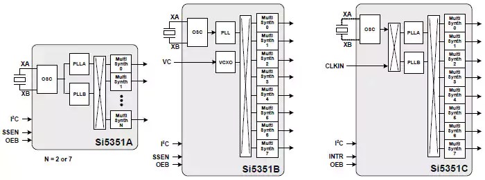
VFO program for Si5351 |
|
Using I2C LCD from: |
|
http://www.amazon.com/Huhushop-TM-Serial-Display-Arduino/dp/B00JM88A94/ |
|
Si5351 library from NT7S. |
|
Uses the updated version of the library (master). |
|
Updated with the format_freq routine from Tom AK2B |
|
|
|
This code is licenced with GNU GPL v2. Please read: https://www.gnu.org/licenses/old-licenses/gpl-2.0.html |
|
|
|
Display library is avaible from: |
|
https://code.google.com/p/u8glib/ |
|
|
|
UNO and 328 boards: Encoder on pin 2 and 3. Center pin to GND. |
|
Leonardo: Encoder on pin 0 and 1. Center pin to GND. |
|
100nF from each of the encoder pins to gnd is used to debounce |
|
The pushbutton goes to pin 6 to set the tuning rate. |
|
|
|
Pin 7 is the RX/TX pin. Put this pin LOW for RX, open or high for TX. |
|
Single transistor switch to +RX will work. |
|
|
|
VFO will NOT tune in TX. |
|
|
|
In serial monitor, you can send "F"+frequency to set frequency. Ex: "F7063000" |
|
|
|
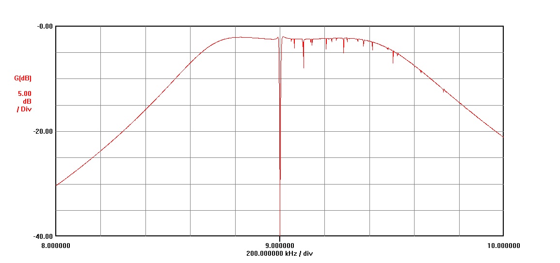
IF frequency is positive for sum product (IF = RF + LO) and negative for diff (IF = RF – LO) |
|
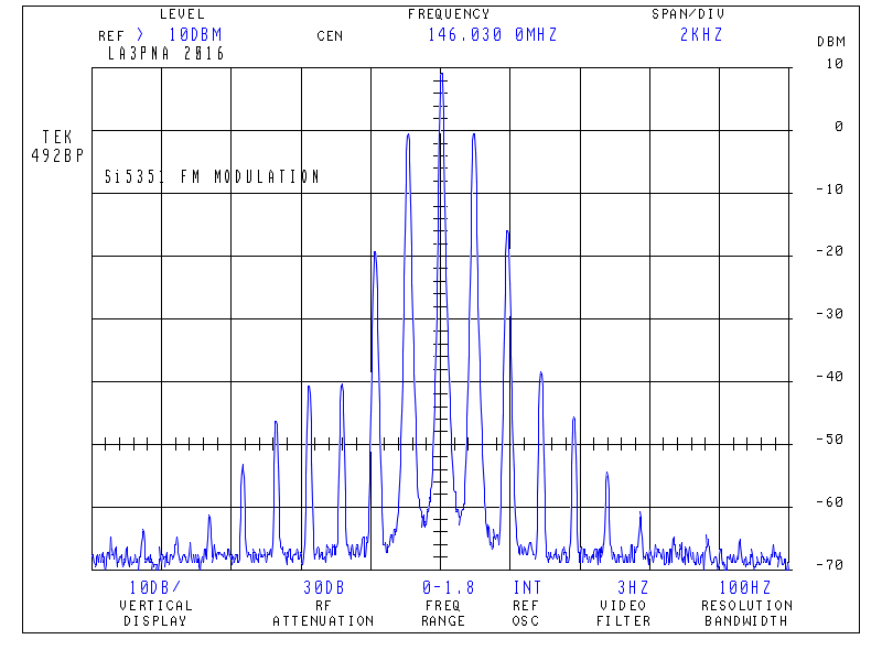
VFO signal output on CLK0, BFO signal on CLK2 |
|
TODO: |
|
* Write own OLED i2c library with optimizing for text to reduce size of compiled program. |
|
*Add variable tuning resolution |
|
*/ |
|
|
|
volatile unsigned long frequency = 144400000; // This will be the frequency it always starts on. |
|
long freqstep[] = {50, 100, 500, 1000, 5000, 10000}; // set this to your wanted tuning rate in Hz. |
|
int corr = 120; // this is the correction factor for the Si5351, use calibration sketch to find value. |
|
long iffreq = 0; // set the IF frequency in Hz. |
|
|
|
#include "U8glib.h" |
|
U8GLIB_SSD1306_128X32 u8g(U8G_I2C_OPT_NONE); // I2C / TWI |
|
String str; |
|
char b[8]; |
|
int inData; |
|
String displayFreq; |
|
boolean A_set = false; |
|
boolean B_set = false; |
|
unsigned int lastReportedPos = 1; // change management |
|
static boolean rotating = false; // debounce management |
|
|
|
#include <si5351.h> |
|
#include "Wire.h" |
|
Si5351 si5351; |
|
// int encoderPinA ; |
|
//int encoderPinB; |
|
#if defined(__AVR_ATmega32U4__) || defined(__AVR_ATmega16U4__) |
|
int encoderPinA = 0; |
|
int encoderPinB = 1; |
|
#endif |
|
#if defined(__AVR_ATmega328P__) || defined(__AVR_ATmega168__) |
|
int encoderPinA = 2; |
|
int encoderPinB = 3; |
|
#endif |
|
bool tx; |
|
int txpin = 7; |
|
int freqsteps = 1; |
|
int bandbutton = 6; |
|
#define arraylength (sizeof(freqstep) / sizeof(freqstep[0])) |
|
|
|
|
|
|
|
void setup() |
|
{ |
|
// set the encoder to inputs |
|
pinMode(encoderPinA, INPUT); |
|
pinMode(encoderPinB, INPUT); |
|
pinMode(txpin, INPUT); |
|
pinMode(bandbutton, INPUT); |
|
// turn on pullup resistors |
|
digitalWrite(encoderPinA, HIGH); |
|
digitalWrite(encoderPinB, HIGH); |
|
digitalWrite(txpin, HIGH); |
|
digitalWrite(bandbutton, HIGH ); |
|
u8g.setFont(u8g_font_courB12); |
|
Serial.begin(9600); |
|
// Initialize the Si5351 |
|
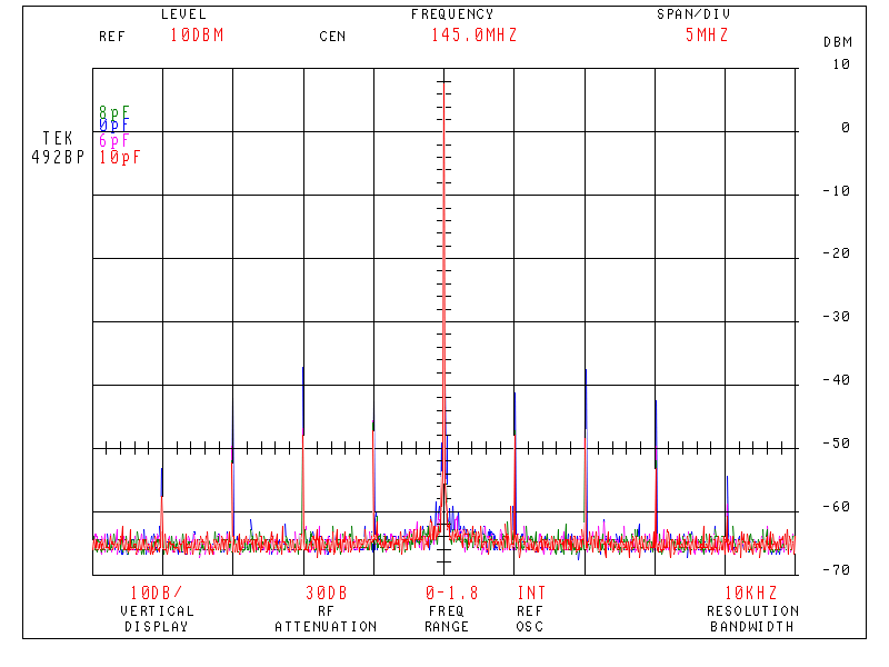
// Change the 2nd parameter in init if using a ref osc other |
|
// than 25 MHz |
|
si5351.init(SI5351_CRYSTAL_LOAD_8PF, 0, corr); |
|
|
|
si5351.drive_strength(SI5351_CLK0, SI5351_DRIVE_4MA); |
|
si5351.drive_strength(SI5351_CLK2, SI5351_DRIVE_4MA); |
|
// assign default color value |
|
if ( u8g.getMode() == U8G_MODE_R3G3B2 ) { |
|
u8g.setColorIndex(255); // white |
|
} |
|
else if ( u8g.getMode() == U8G_MODE_GRAY2BIT ) { |
|
u8g.setColorIndex(3); // max intensity |
|
} |
|
else if ( u8g.getMode() == U8G_MODE_BW ) { |
|
u8g.setColorIndex(1); // pixel on |
|
} |
|
else if ( u8g.getMode() == U8G_MODE_HICOLOR ) { |
|
u8g.setHiColorByRGB(255, 255, 255); |
|
} |
|
|
|
#if defined(__AVR_ATmega32U4__) || defined(__AVR_ATmega16U4__) |
|
encoderPinA = 0; |
|
encoderPinB = 1; |
|
//Code in here will only be compiled if an Arduino Leonardo is used. |
|
// encoder pin on interrupt 2 (pin 0) |
|
attachInterrupt(2, doEncoderA, CHANGE); |
|
// encoder pin on interrupt 3 (pin 1) |
|
attachInterrupt(3, doEncoderB, CHANGE); |
|
#endif |
|
#if defined(__AVR_ATmega328P__) || defined(__AVR_ATmega168__) |
|
encoderPinA = 2; |
|
encoderPinB = 3; |
|
//Code in here will only be compiled if an Arduino Uno (or older) is used. |
|
attachInterrupt(0, doEncoderA, CHANGE); |
|
// encoder pin on interrupt 1 (pin 1) |
|
attachInterrupt(1, doEncoderB, CHANGE); |
|
#endif |
|
si5351.set_freq((iffreq) * 100ULL, SI5351_CLK2); |
|
|
|
} |
|
|
|
|
|
void loop() |
|
{ |
|
tx = digitalRead(txpin); |
|
rotating = true; // reset the debouncer |
|
|
|
if ( lastReportedPos != frequency) { |
|
lastReportedPos = frequency; |
|
// Serial.print(frequency); // unncomment this to output frequency on change. |
|
si5351.set_freq((frequency + iffreq) * 100ULL, SI5351_CLK0); |
|
} |
|
|
|
if (digitalRead(bandbutton) == LOW ) { |
|
delay(150); // delay to debounce |
|
if (digitalRead(bandbutton) == LOW ) { |
|
freqsteps = freqsteps + 1; |
|
Serial.print(freqstep[freqsteps – 1]); |
|
Serial.print(" "); |
|
Serial.print(freqsteps); |
|
Serial.print(" "); |
|
Serial.println(sizeof(freqstep)); |
|
if (freqsteps > arraylength – 1 ) { |
|
freqsteps = 0; |
|
} |
|
delay(1000); //delay to avoid many steps at one |
|
} |
|
} |
|
format_freq(); |
|
|
|
|
|
// rebuild the picture after some delay |
|
delay(50); |
|
|
|
if (Serial.available() > 0) // see if incoming serial data: |
|
{ |
|
inData = Serial.read(); // read oldest byte in serial buffer: |
|
} |
|
if (inData == 'F') { |
|
frequency = Serial.parseInt(); |
|
inData = 0; |
|
} |
|
} |
|
|
|
|
|
// Interrupt on A changing state |
|
void doEncoderA() { |
|
// debounce |
|
if ( rotating ) delay (1); // wait a little until the bouncing is done |
|
// Test transition, did things really change? |
|
if ( digitalRead(encoderPinA) != A_set ) { // debounce once more |
|
A_set = !A_set; |
|
// adjust counter + if A leads B |
|
if ( A_set && !B_set ) { |
|
if (!tx) { |
|
frequency += freqstep[freqsteps]; // hehre is the amount to increase the freq |
|
} |
|
rotating = false; // no more debouncing until loop() hits again |
|
} |
|
} |
|
} |
|
|
|
// Interrupt on B changing state, same as A above |
|
void doEncoderB() { |
|
if ( rotating ) delay (1); |
|
if ( digitalRead(encoderPinB) != B_set ) { |
|
B_set = !B_set; |
|
// adjust counter – 1 if B leads A |
|
if ( B_set && !A_set ) { |
|
if (!tx) { |
|
frequency -= freqstep[freqsteps]; // here is the amount to decrease the freq |
|
} |
|
rotating = false; |
|
} |
|
} |
|
} |
|
void format_freq() { |
|
u8g.firstPage(); |
|
do { |
|
u8g.setPrintPos(0,15); |
|
uint16_t f, g; |
|
f = frequency / 1000000; |
|
if (f < 10) |
|
u8g.print(' '); |
|
u8g.print(f); |
|
u8g.print('.'); |
|
f = (frequency % 1000000) / 1000; |
|
if (f < 100) |
|
u8g.print('0'); |
|
if (f < 10) |
|
u8g.print('0'); |
|
u8g.print(f); |
|
u8g.print('.'); |
|
f = frequency % 1000; |
|
if (f < 100) |
|
u8g.print('0'); |
|
if (f < 10) |
|
u8g.print('0'); |
|
u8g.print(f); |
|
u8g.setPrintPos(80,32); |
|
u8g.println(freqstep[freqsteps]); |
|
if (tx) |
|
{ |
|
u8g.drawStr( 110, 15, "TX" ); |
|
} |
|
//draw(); |
|
} while ( u8g.nextPage() ); |
|
} |