Homemade thermal test chamber

Some time back (2016 timeframe) I built a test chamber out of an inexpensive freezer, after having several project that required taking some thermal data over the expected useable range.  I was looking for a used laboratory freezer that goes down to -60° or lower, but none seems available used.

IMG_1528

The freezer uses “pentane C” cooling media,  and the initial test suggested that before modification, the freezer, with the pump running all the time would go down to -26°C.

After confirming that the freezer would work, it was time to void the warranty. What better way, than by drilling a hole through the side of the freezer?

IMG_1530

I choose to drill through the plastic with a small pilot drill, then poke around to see if there was any cooling tubes in the side. That way I hopefully I would be able to avoid cutting any of the tubes.  Given that I couldn’t feel anything in the foam insulation, it was time for the hole saw.  With a hole through the side of the bottom compartment, a 36mm plastic tube was fitted, some foam spray was used to fix the defects and some clear silicone sealed the gap between the tube and the side of the freezer.

The idea I started with was to make a proper, insulated patch panel, with both coax and DC connectors, but after some thinking, the tube filled with a rag seemed like a more flexible approach.

IMG_1536

Ripping out the thermostat and sensor tube was quite easy, threading the sensor cable for a ready-made 1-wire sensor (got this via bobcatinabox.com some time back). Drilling a hole in the wall of the  small compartment was done by poking through the insulation from the back with a pice of wire, then when confirming it was clear off the cooling tubes and drilling through.

A 12V PTC heater with fan was modified so that the fan can run all the time, and fitted to the shelf. This way there will be constant air circulation inside, and the heater can be controlled by the microcontroller.

On the back of the freezer,  the connector block for the freezer had an unused terminal that was repurposed as a terminal for the live wire that before had gone to the thermostat. A 12V 20A switch mode power supply was added, and fixed to the back wall with a couple M3 screws and nuts.

IMG_1542

A Arduino was fixed above the power supply, and a small pice of wearoboard with some relays and driver transistors to switch the power to the pump motor and to the heater.

The program running on the microcontroller is a fuzzy logic implementation with a 2°C hysteris. There is also some timing logic to not turn on the pump before the back pressure has bled trough, or the fuse will blow.  I started out with some SCR’s but the cheap eBay SCR I bought had too much loss before it caught fire.

The program can be found here: https://github.com/la3pna/thermal-chamber

I intend to implement a proper dual PID for the controller one day, as keeping temperatures within 0.5°C should not be too difficult. Adding network interface in addition to the USB and a propper way of handling those messages would make it more versatile.

There is currently no cap on how hot it can become inside, but I suspect the plastic casing will not take well to having it run at high temperature for long time.

The inside usable size is approx 320x320x180mm, so there is no way of fitting a 19″ rack in there, but for smaller parts, it will do OK.  Now I just need to build the multiple termocouple amplifiers into a box with some method of reading it out.

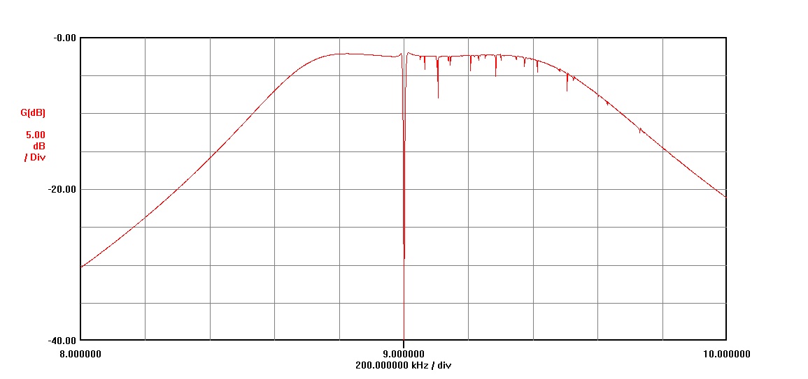
An example of measured data:

tcxo


Mitsubishi MOSFET VHF hybrids

Observe that Mitsubishi has EOL’ed (End Of Life) most of  their MOSFET range as of Jan 1. 2019

The last 15 years there have been a large development in MOS hybrid preformance, combined with a reduction in price, making these hybrid amplifiers quite a reasonable choice for a power amplifier in a VHF or UHF transceiver.

This hybrid is the Mitsubishi RA07H0608M made for the 60-88MHz range. I have been using these for experiments in the 70MHz band with both linear modes and FM. This hybrid should work on 50MHz, but determining the optimal bias point for linear would require the ability to do 2-tone testing.

I managed to burn out one of the amplifier modules due to self oscilations, and wanted to do some reverse engineering of what’s in the hybrid.

This hybrid is  a thick film hybrid with 2 MOSFET dies, one for the PA and one for the driver in addition to biasing and impedance maching components. The white goop is probably non-acidic sillicone used to attach the plastic casing to the substrate and cooling tab.

module.png


The driver amplifier is a vertical MOS die, approximately 1mm x 2mm in size and with 2 bond wires to the base, and 3 to the drain.

driver_transistor

The PA transistor is a fairly large vertical MOS device, with 2 clearly visible trenches and several bonding wires on the drain. This is to reduce the inductance in the bonding wire and carry enough current. The die is quite large, approx 3mm x 3mm in size. There are some interconnections on the top of the die, but due to the passivation and sillicone around the die, its difficult to see the connections clearly.

PA_transistor.png

A interesting thing is how one pass wires over antother. The hybrid consists of  a ceramic base (called substrate), with a groundplane on the backside that are bonded to the cooling tab. Traces is then put on the top of the ceramic substrate and fused together by firing. In order to make a wire pass over another, the  bottom wire is laid down and fired (heated in a furnace to a given temperature), then a isolating layer is laid down and fired before the other trace is laid down and fired. This is done because there is only one layer avaible to put traces on, and having extra wire connections to the hybrid is expensive. The opague isolator as shown are probably BeO, although the datasheet don’t mention that there is BeO in the device. BeO dust is toxic.

The traces shown here is  the bias line to the PA FET passing over the drain supply to the driver FET.

pa_pass.png

Another interesting thing about this hybrids are the extensive use of 0402 and 0603 resistors and capacitors. With thick film hybrids, its quite possible to put the resistors directly on the substrate. A reason to not do that in a amplifier like this may be that the resistors will have a termal gradient and that the resistors would require expensive laser trimming.  High value capacitors like those used for decoupling are hard to make on a hybrid like this, so soldering in regular SMD components, and even electrolytics some times.

The PA FET has negative feedback to reduce gain and improve stability, while I could not see any for the driver. There seems to be some damage to my module there, could I have blown that off the hybrid? The increase in drive level by adding some light feedback to the driver may be worth a experiment.

The output and input matching looks to be of the lowpass kind, and on the output there are some harmonic supression. The RF design here clearly outperforms the mechanical and cooling. Interfacing these modules into circuits that once held older bipolar hybrids may not be straigth forward. There is a lot of gain to several GHz avaible in the FET’s and the grounding needs to be good to avoid oscillations.

Overall, the reverse engineering of these modules were quite interesting.  A interesting thing to do may be to trace out the shcematic, although it should look like most any of the other modules available. Curve tracing the FET could be interesting to determine their parameters.

A notch filter for phase noise measurment

Measuring phase noise is difficult, due to the large difference between the signal and the noise.  Here I will outline the method I use to determine the noise of a oscillator and show the basic bandpass – notch filter used to reduce the carrier level to a level that the common spectrum analyzer can handle.   The filter shown here will be made for 9MHz, but other frequencies can be realized as long as high Q matched crystals can be found.

When doing these measurements, reducing the noise figure of the spectrum analyzer, and knowing the inserted gain is important. I use a module with a ERA-2 MMIC mounted in a die cast box with extended filtering on the DC input.

The filter module start with a QTC (Quad Tuned Circuit) mixed form bandpass filter.  This is built and tuned for a flat bandpass before the notch

QTC_9MHz

After the filter is built and tuned the crystals are connected over the 2 resonators in center and the filter is adjusted to have a as flat as possible passband. This way, with crystals matched as close as possible (2Hz) the notch depth should be better than 80dB. If the crystals can’t be matched, then a trim capacitor can be placed in series with the crystal, but this makes the tuning of the notch depth much more difficult.

QTC_9MHz_notch

The obtained filter does not need to have the notch in the center of the passband. the 3dB points of the filter will be what limits the bandwith of your measurement. If the crystals have high Q and no spurious responces (mine had some) then the passband should be flat. If there is some spurious responces, you can average it out on most spectrum analyzers. Knowing the width of the notch at the 3dB point determines how close to the carrier you can measure the phase noise.

notchfilter

To use the filter with a spectrum analyzer, you add a low noise amplifier with known gain at the frequency you operate on between the filter and the spectrum analyzer. Add a variable attenuator in front of the filter and set this to max attenuation before connecting it to the signal source.

Tune the signal source to the frequency where it is attenuated the most by the filter and reduce the attenuation to 0. If The noise level around the notch should be somewhat higher than the attenuated carrier.

If the spectrum analyzer have a marker that can show the amplitude level in dBm/Hz then the level of the phase noise in dBc is: Source output power(dBm) + noise amplitude (dBm) + (loss through filter in dB) – (amplifier gain in dB). For example, lets assume my source is at 10dBm, the measured noise level at -115dBm,  2.4dB filter loss and 20dB gain:  10dBm + (-115dBm/hz) + (-2.4dB) –  (20dB) = -127dBc/Hz phase noise.

If the analyzer does not have a marker function then you need to know the bandwith of the IF filter in the analyzer in addition to the parameters above.  The total equation would then be: Source output power(dBm) + noise amplitude (dBm) + (loss through filter) – (amplifier gain) – 20*log(analyzer bandwith in Hz ).   For example, source at 10dBm, measured noise level at -105dBbm in 100Hz bandwith, 2.4dB filter loss and 20dB gain: 10dBm + (-95dBm) +(-2.4dB) – (20dB) -(20*log(100)) = -147dB/Hz phase noise.

block_phasenoise

Accurate noise measurements are not easy to do. Careful evaluation of all used components and careful measurements with averaging of the traces helps to obtain accurate measurements. Alternative methods use phasing or PLL methods, and have better accuracy over a larger bandwidth, at the expence of a more advanced measurement setup.

Update 1.th February 2015:

Did a measurement of the HP8656B signal generator using the notch filter and a ERA-2 amplifier with 15.7dB gain:

notchfilter_9MHz_HP8656B


The input signal into the notch filter were 0dBm and the notch filter loss 2.4dB. The total equation will then be: 0 +(-106.1dBm/Hz) + (-2.4dB) -15.7dB = -124.2dBc/Hz at the point 10KHz offset from the carrier.  This value corresponds well with other methods used to measure the phase noise on this generator. The value is 10dB better than the than what the datasheet states as worst case phase noise, not uncommon for HP equipment from the 1980s era.

IMD measurment generator

IMD or Intermodulation distortion testing is in RF systems usually done with 2 signal sources, quite close in frequency, and one determines the level of the unwanted responses. The actual measurement procedure is shown quite well other places in the literature [1].

Here I will show my design for an high performance crystal controlled RF source delivering 100mW or so into 50 ohm at HF. The obtained phase noise from this generator are better than the resolving bandwidth of my phase noise measurement -140dBc so there should not be any problems from the phase noise of the signals.

final_schematic

The oscillator circuit used is an common base Butler circuit, as described in Matthys [2]. There are a total of 5 frequency dependent components, the crystal, the inductor, and 3 capacitors. The oscillator have limiting to reduce the oscillation amplitude and to improve the frequency drift.

values

C5+C8 is selected such that the middle value falls in the center of the trimmer C5 range. The chosen crystal should be an HC49 size, not one of the smaller models, as those tend to drift more than their larger counterparts. Measured drift for this oscillator on 3.7MHz is less than 10Hz from start (red trace). Crystals can be ordered from [3] or [4]. Crystal ovens are not recommended, if temperature drift is a problem, fit the crystal with an Styrofoam bead to insulate.

grr_drift

The oscillator is followed by an 3. order low-pass filter to remove harmonic products from the limiting of the oscillator. There exists several types of filter one can use if one wants, I have calculated the values for an half wave filter. This have the simplicity of calculation that the reactances of the components are equal to the system impedance. In this case, for an given frequency :

formula1
where f is the crystal operating frequency in Hz. Different filter topologies like Chebychew or Butterworth can be used to improve the harmonic attenuation of the filters. Information on the calculations of such filters can be found in [1]

Following the filter is an attenuator that can be inserted if the max output level is higher than the desired operating amplitude. Suitable attenuator values can be found several places on the internet. If not used, insert an 0 ohm resistor into R8.

The attenuator is followed by an variable gain hybrid cascade amplifier. This consists of an cascade of an J-fet (MMBT310) and an bipolar transistor (BC847). The J-fet is impedance matched to the 50 ohm system with an balun made by winding 4 turns bifilar on an BN-43-2402 ferrite binocular core. The output is in an similar way matched to the power amplifier with an transformer wound on an BN-43-2402 core. The primary side against the hybrid cascade consists of 12 turns, the side against the power amplifier consists of 2 turns. Wind these such that the leads protrude on each side of the core. The amplifier gain can be adjusted with the trimmer R11 such that the output amplitude is at an fixed level, or this can be taken to an potentiometer mounted in the box such that the output power can be varied if needed.

The power amplifier consists of an NE46134 medium power RF transistor, operating in class AB and delivering a nominal 100mW output power. The inductor is wound on an FT37-43 ferrite core, and 10 turns should suffice for all HF frequencies. Following this is an 5.th order low-pass filter. This filter uses the same capacitor and inductor values as calculated for the 3. order filter before. Observe that C23 is double the value of the other capacitors. The inductors should be wound on iron core toroids. T37 size is recommended. -2, -7 and -10 material should fit the frequency range from 2MHz to 50MHz.

IMD_source_plot

final_board

The PCB for this design is available from OSHpark:

https://oshpark.com/shared_projects/trtilfzL  3 boards for $36 with delivery worldwide.

The PCB have 2 small isolated holes on each side of the crystal and transformer to secure those to the PCB. The PCB is made to fit inside an Hammond 1590B die cast enclosure. All the used components are 0805 size. 1206 should fit, although a bit large.

In order to combine the generators, some kind of combiner is needed. There exists several kinds of couplers that are common to combine generators. 6dB hybrids are easy to construct and work over an large frequency range. For an small bandwidth range, like these crystal controlled oscilators, an Wilkinson divider gives 3dB split, and are easy to construct.

The PCB for the Wilkinson splitter can be ordered from OSHpark:

https://oshpark.com/shared_projects/9O4qDXVJ 3 boards for $9.90 with delivery worldwide.

wilkinson

A limited amount of kits may be available from me. Documentation and PCB files available on request.

[1] Hayward et. all, Experimental methods in RF design (EMRFD).
[2] Matthys, Crystal oscillator circuits.
[3] Expanded spectrum systems http://www.expandedspectrumsystems.com/prod4.html
[4] ICM https://www.icmfg.com/

open T-check

As of 24 mar 2018, I will no longer do any updates to the T-check program, I reccomend you try out KE5FX’s GPIB toolkit, as this has a similar program.

Ok, since this blog seems to be about the software I write, and not about RF engineering, altough this may be related.

T-check is an routine by R&S to verify the validity of network analyzer SOLT calibration.  This is explained in the R&S application note 1EZ43_0E, covering the math behind the routine as well as the T-checker, an coaxial adapter with an integrated 50 ohm resistor. An simplified method to realize this may be an T adapter with an 50 ohm termination on the 3. port.

t-check

The VNA is calibrated and this device is inserted instead of the DUT. The S-parameters are then saved and run through the T-checker program.

t-check

The program, as supplied from R&S does only work on 32bit computers.  I made an implementation that run on both 64bit and 32bit windows as well as linux, BSD, UNIX, OSX and even Playstation 3 with MONO.

My implementation, named “open T-check” are avaible here

First post

So this is my “new” blog, altough the domain have excisted for a while, I have not done any blog post yet. My former blog was on blogger.com, before they messed up, and the resulting mess ended up with no pictures, and posts with scrambled text. Most of the content was less interesting, so the relevant parts may end up in an post here.

In this blog I plan on sticking to RF (Radio Frequency) engineering, with some de-tours into other fields, mainly electronics.  I will try to write all my post in english, but there may appear some isolated posts in norwegian from time to time.   I have an goal to keep the blog free of any comercial avertizing. As of now, I’m not paid by any of the mentioned firms in my posts, if that changes, I will make sure to blog about it.

I’m considering getting an domain for this blog, but for now, I’l use wordpress as the publishing platform.